Thermography on the Trail of the Fault
Today, thermographic damage and function analysis of electronic components is an established test method in electrical engineering. This method is also used for research purposes at the Institute for Electrical Systems and Energy Logistics at BTU Cottbus-Senftenberg. In this context, Prof. Dr. Ralph Schacht is intensively involved with the material and system characterisation as well as the non-destructive failure analysis of printed circuit boards, electronic components, microelectronics as well as composite systems of packaging and interconnection technology.

Non-destructive testing (NDT) – in contrast to destructive component testing – implies that the test application must not influence or reduce the usability of the test object in any way. Thermal imaging is a non-destructive, very efficient method. It enables the imaging detection of thermal radiation as well as the interpretation of the observed surface temperatures.
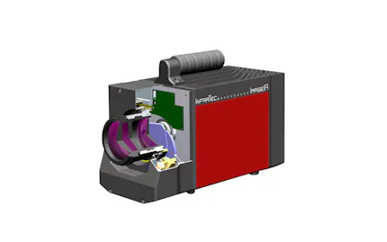
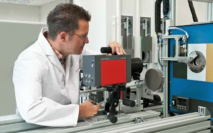
At the Institute of Electrical Systems and Energy Logistics at the BTU Cottbus-Senftenberg, non-destructive component testing is carried out using various thermography methods: passive IR thermography, active IR pulse thermography and active IR lock-in thermography. The infrared camera used for this purpose is the ImageIR® 8300 from InfraTec with a M=3x magnification microscope lens or a macro attachment. The measurements are evaluated with the IRBIS® 3 thermography software belonging to the camera and the additional module IRBIS® 3 active.
InfraTec Solution
Brandenburg University of Technology Cottbus-Senftenberg (BTU);
Institute for Electrical Systems & Energy Logistics
www.b-tu.de/fg-schaltungstechnik/
Prof. Dr.-Ing. Ralph Schacht
Thermographic System:
ImageIR® 8300
Passive IR Thermography
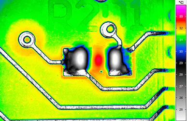
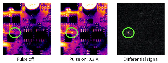
With this method, electrical "short-circuit currents" are selectively injected into the assemblies to be tested. This can lead to increased current flows in faulty areas, which in some cases trigger the slightest temperature changes there and can be detected using thermography. Short-circuit tests of electrical through-hole platings in printed circuit boards (PCB) serve as an example here. Due to the possibility of evaluating the differential image within the IRBIS® 3 thermography software, the contact point can be precisely localised in real time (Fig. 1).
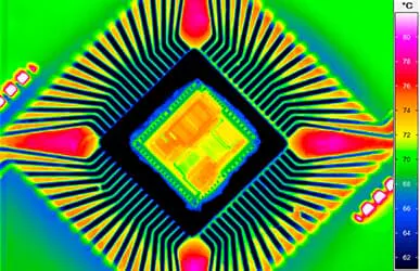
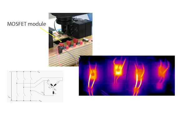
The utilisation of, for example, power MOSFETs in 3-phase inverter operation can also be displayed and monitored very well using this method (Fig. 2). With the aid of the high-resolution M=3x microscope lenses used on the ImageIR® 8300 infrared camera, it is possible to characterise integrated passive components at wafer level. The thermal behaviour of nickel-chromium resistors as a function of their power dissipation was analysed here (Fig. 3).

Active IR Pulse Thermography
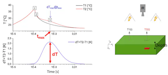
This form of non-destructive testing is a frequently used method to detect hidden damage in components. Heat is pulsed into a sample while the temperature field of the stimulated surface is observed in parallel. This enables the evaluation of both heating and cooling curves. The advantage of impulse thermography is its high speed and, as a result, the high potential for a 100 percent inspection during a production process.
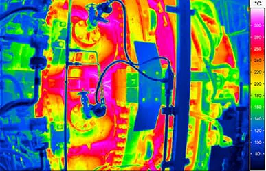
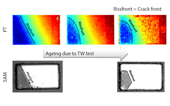
Using this method, it is possible to take advantage of the fact that locally different cooling processes occur after the excitation impulse. The time of the maximum temperature difference and the difference as such are determined. This method also allows conclusions to be drawn about structures that are not directly located on the component surface (Fig. 4).
Practical examples of this measurement method can be seen in connection with the assembly of power semiconductors. Delaminations in a solder layer after cyclic loading or the propagation of crack fronts in sintered layers can, for example, be detected.
Active IR Lock-in Thermography
The lock-in principle or lock-in amplification is employed when a useful signal is to be found in a statistically noisy overall signal. This must be periodically amplitude-modulated in a targeted manner. In the simplest case, this is done by switching the supply voltage of an electronic component on and off or by sinusoidal modulation.
In addition, this method allows very small and weak heat signals to be detected. Taking, for example, a test structure with a 50 µm small diode and exciting it with 10 mW at 0.1 Hz (duty cycle 50 %), the sought-after measurement signal in the pure thermal image is below the detection limit. However, the power dissipation source can be localised very clearly via a generated amplitude image – even in real time using the IRBIS® 3 active thermography software.
Lock-in thermography is also excellent for localising crack tips or measuring crack lengths by the appearance of the thermoelastic effect in the phase image (Fig. 5).
ImageIR® 8300 - High Thermal Resolution for Precision Measurements
The BTU Cottbus-Senftenberg has been using the ImageIR® 8300 for the measurements presented here for several years. This camera is equipped with a 25 mm standard lens as well as M=1x and M=3x magnification microscope lenses. Internally, two filter-aperture wheels have also been installed, a unique feature of the camera series, with which both signal-attenuating filters and spectral filters can be swivelled in remotely in parallel. In addition to the high spatial resolution of this system, excellent measurement accuracies are also achievable with each lens, so that exact and repeatable results are obtained.
The associated IRBIS® 3 active software allows, among other things, convenient data evaluation options of image sequences, the calculation of phase and amplitude images as well as the analysis with various methods of active thermography. These include, for example, the quotient method, pulse phase and lock-in thermography.
The ImageIR® 8300, including its software tools, has become an indispensable aid in scientific training as well as in research work at the institute.

