
Thermography in the Electronics & Electrical Industry
Invisible defects, hotspots, unstable prototypes? Our thermography systems make even µm structures and µK differences visible— contactless, fast, and precise. Ideal for development, failure analysis, or inline quality assurance.
InfraTec Cameras and Systems for Electronics
Get maximum IR resolution – large & small test objects: detectors with up to (2,560 × 2,048) IR-pixels; pixel resolution < 1µm
Measure the smallest temperature differences – precisely & innovatively: < 0,015 K; with Lock-in therrmography down to the µK range
Detect the shortest reactions – fast & synchronous: up to 105 kHz, trigger, 10 GigE
Benefit from customized solutions – modular & scalable: lenses, software, complete test stations


")


Non-contact Measurement in Electronics with an Infrared Camera
The thermographic inspection of electronic components and assemblies is an established test procedure for failure detection and quality management – from the development of first prototypes to serial production.
Areas of Application for Thermal Imaging in Electronics
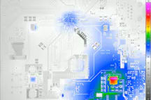
Electronic failure analysis for hotspot detection
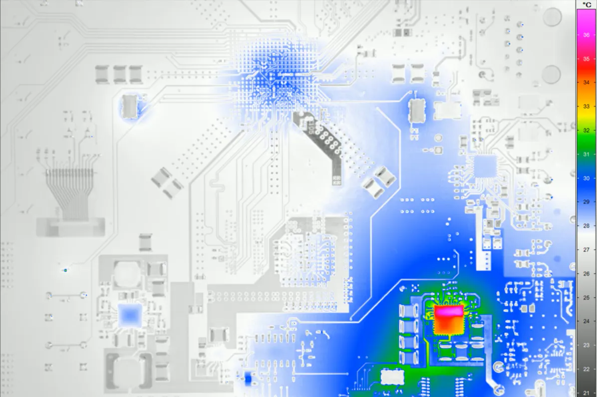
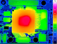
Thermal Mapping, measurement of atypical temperature distributions on the surface of printed circuit boards, integrated circuits, and multichip modules to detect connection faults and defective components
Thermal design
Thermal management, temperature-time behavior, board layout, analysis of cooling concepts, thermal design process
Service life analysis
Analysis of temperature behavior during load cycles as well as during switch-off and switch-on cycles, investigation of thermal aging, and validation of simulation calculations related to self-heating
Inline quality assurance in electronics manufacturing
Versatile tool for quality assurance of process parameters and products during production
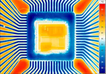
Diagnostics for Power Electronics Systems
Development of inverters for photovoltaic systems, charging stations, switchgear, and industrial drives.
Thermography Allows the Detection of
elevated contact resistance,
higher impedance caused by cable constriction
hidden cracks in connection points,
power losses due to high frequency (HF) mismatch,
faulty thermal connections of heat sinks,
short circuits, soldering defects such as cold solder joints,
thermally active watermarks as a protective measure against cyberattacks in the hardware and software area
design of boards and testing of cooling concepts
Advantages of Thermal Imaging in these Fields of Application
Safe temperature measurement even on live parts
Complete recording of the temperature distribution and its temporal progression of complex assemblies during operation
Does not affect the high frequency (HF) impedance of the test object or the heat dissipation from it, which helps to reliably avoid corresponding measurement errors
Clearly determining temperature differences in the µK range
Information on thermal characteristics of components and circuits as early as the design phase


Lock-in Thermography: Clearly Determine Temperature Differences in the µK Range
Thermal imaging has become a standard procedure in electronics. With increasing miniaturization and ever lower supply voltages, failure analysis is becoming more complex. Classic infrared cameras with resolutions of up to < 20 mK are sufficient in many cases, but they do have their limitations.
Lock-in Thermography is used to detect minute temperature differences in the µK range. In this process, the test object is analyzed non-destructively using periodic excitation. When using the lock-in method, the measurement time increases significantly compared to real-time measurement as the desired resolution increases and can take several minutes. It is therefore particularly helpful if such measurements can be made in one step using a large-format, high-resolution camera.
Benefits at a Glance:
Highest sensitivity: detect temperature differences in the µK range
Non-destructive analysis: Reliably detect even deeper-seated defects through periodic excitation
Optimal results for complex components: Thanks to large-format, high-resolution cameras
Improved efficiency: Less stitching (combining partial images into a complete thermogram), less effort, lower costs
Detection and allocation of faults in the µK range


Electronics and Semiconductor Module Testing by means of Lock-in Thermography
Find out in our white paper how you can use lock-in thermography to detect faults in electronic and semiconductor components. Benefit from our practical tips and achieve the best possible measurement results with the E-LIT test bench from InfraTec.


Fields of Application for Thermography in Electronics Testing
Thermography is now a key tool in electronics development and manufacturing. It helps engineers and quality managers visualize heat distribution, identify sources of error at an early stage, and ensure the reliability of electronic assemblies. From the initial design phase up to series production, it provides valuable information for stable processes and high-quality products.
Electronic Failure Analysis and Hot-spot Detection
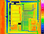
Failure analysis using thermography is essential for investigating the causes when the function of electronic products is impaired or safety-related problems occur. Infrared cameras allow accurate identification of atypical temperature distributions, both in terms of area and spatially. When high-resolution cameras are used in conjunction with lock-in thermography, even the slightest temperature differences in the µK range can be measured. High geometrical resolution enables analysis up to the smallest details.
Examples of Applications for Electronic Failure Analysis
Reliable detection of increased resistance during heat transfer
Detection of thermal anomalies in integrated circuits and their precise localization
Locating short circuits and other defects
Perform electronic circuit testing on integrated circuits, electronic circuits and power electronic circuits for hot spots
thermos optical failure analysis in PCB design in the event of overheating
3D depth analysis of faults in multilayer printed circuit boards and multi-chip modules by adjusting the lock-in frequency
Electronics testing to identify thermal bridges, overheating, and other anomalies in electronic devices and circuits
Advantages of Thermal Imaging in Failure Analysis
Early detection of defects and safety-related weak points
Full-surface visualization of atypical temperature distributions in real time
Non-destructive analysis even for sensitive or complex assemblies
High precision up to the µK range thanks to lock-in thermography
Rapid localization of the cause instead of merely measuring symptoms


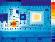
Thermal Design – Thermal Management Layouting
Thermal design of electronic components is a key factor in the development of new chip technologies and applications in power electronics. Thermography can be used for thermal mapping (the spatial acquisition and evaluation of the temperature distribution on electronic components) to identify components with excessive heat generation and mutual thermal interactions between components at an early stage. As a result, early adjustments to prototypes can significantly reduce development costs.
Examples of Applications in Thermal Management Layouting
Analysis of temperature development and heat dissipation in PCB (printed circuit boards) design
Sensible arrangement of components
Determination of the optimal operating points of components
Optimization of energy processing in the field of power electronics
Improvement of heat distribution in switching power supplies and power supply systems
Development of strategies for cooling and heat dissipation under real conditions
Thermal management for quality assurance
Validation of simulation calculations for self-heating of electronic objects
Advantages of Thermography in Thermal Design
Full-surface display of temperature distribution instead of selective measurement helps to ensure that errors are not overlooked
Non-contact and non-destructive, even with sensitive components
High temporal resolution to visualize dynamic heat processes


Service Life Analysis
When developing new electronic components or assemblies, there is initially no application-specific data or information available on service life and performance losses. Predicting these parameters as accurately as possible can be a decisive competitive advantage. Manufacturers and developers therefore carry out complex temperature or load cycle tests to simulate the aging of electronic components.
The high reliability of InfraTec’s infrared cameras really pays off, especially during 24/7, long-term and reliability tests. The programmed measurement sequences for long-term and stress tests can be stored directly in the camera's internal memory. Add-ons to the IRBIS® 3 analysis and evaluation software also enable the use of programming and development environments that support real-time data acquisition and signal processing.
Remote control reduces sources of interference such as camera shake when touching the camera.
Examples of Applications in Service Life Analysis
Analysis of temperature development during electrical, thermal, or mechanical stress tests on and around electronic objects
Measurement of temperature-time behavior during long-term tests


, consisting of GaN")
Advantages of Thermal Imaging in Service Life Analysis
Early prognoses on the service life and performance losses of electronic components
Realistic simulation through temperature and load cycle tests
Complete documentation of temperature-time curves during long-term tests
High reliability in continuous operation (24/7) for valid results
Reduction in costs and risks, as weak points are identified before market launch
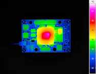
In-line Quality Assurance in Electronics Manufacturing
In electronics manufacturing, thermographic temperature measurement is used as a versatile tool in quality assurance.
Application Examples in Electronics Manufacturing
Permanent monitoring of critical technological parameters
Inline inspection of products in production
Final functional testing
Advantages of Thermal Imaging in Electronics Manufacturing
Inline quality control by comparing with a flawless reference model (Golden Board) during production without interrupting the process
Early failure detection → lower rejection rates, increased process stability
Contactless analysis, even on sensitive or live components
Fast end-of-line analysis for reliable product release
Continuous thermo optical process monitoring of critical parameters for reproducible quality

Diagnostics for Power Electronics Systems
Thermography is frequently used in the development of power electronic components to detect overheating caused by faults, high power losses, or aging effects. Power electronic components such as inverters can be monitored safely during operation using thermography.
Application Examples for Power Electronics Diagnostics
Applications in:
PV system inverters
Charging stations
Switchgear, power supplies, and switching power supplies
Industrial inverters
Drive inverters
Special Considerations in the Development of Electric Drives
Power electronics are also a central component of drives in electric vehicles – where drive inverters (also known as traction inverters) convert battery DC into AC for the motor and enable the recovery of braking energy – or in industrial drives, for example, as inverters for speed control.
The use of modern power semiconductors made of silicon carbide (SiC) and gallium nitride (GaN) allows for further increases in the efficiency of drive inverters, lower switching and power losses, and more compact designs. These materials, also known as wide-bandgap (WBG) semiconductors, offer significant advantages over silicon (Si) in power electronics – particularly in terms of efficiency, switching speed, power density, and temperature resistance. A particularly important advantage of WBG semiconductors is their high voltage withstand capability, making them especially suitable for use in high-voltage applications.


The use of SiC, GaN, and other WBG semiconductors presents several unique challenges for thermography. The components
are significantly smaller,
switch faster, and
have higher current and power densities.
For thermal diagnostics, thermographic cameras with high spatial resolution and macro- or micro-optics are necessary, as hotspots cannot otherwise be sufficiently isolated. Due to the high switching frequencies, thermal effects are often only measurable with very short integration times. Many WBG materials also exhibit low emissivity, and the emissivity levels of components located close to one another can differ significantly from one another in some cases. Therefore, high-end cameras and comprehensive expertise are required for the diagnosis of modern power electronics.
Other faults in power electronics that manifest as thermal effects – such as uneven temperatures on heat sinks, connection errors, or overloaded traces – are much easier to detect.
Advantages of Thermography for Diagnosing Power Electronics
Non-contact and safe diagnosis, e.g., of critical gate temperature, even on sensitive or live components
No interference with the circuit during measurement
Analysis during operation under real load conditions
Early detection of thermal anomalies (ideal for preventive maintenance) and trend analysis
Investigation of highly dynamic switching processes, e.g., using pulse width modulation (PWM) in microcontrollers
Easy comparison of identical components
High-performance Thermography Systems by InfraTec

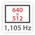
up to (2,560 × 2,048) native IR pixels for analysis of complex assemblies – 16 times the resolution of standard VGA cameras with (640 × 512) pixels
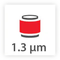
with pixel resolutions of less than up to 1.3 µm with InfraTec's microscopes and even less than 1 μm using SIL lenses
allow easy manipulation of the DUT (Device Under Test) during measurement
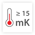
between defective and intact structures in the range of a few microkelvins due to high thermal resolution up to < 0.015 K or in the µK range in combination with the lock-in method
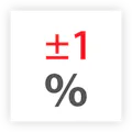
of up to ± 1 °C or 1% for reliable measurements and comparability
Analysis of very fast temperature pulses in full-frame format or up to 105 kHz in partial-frame mode
Optimal setup for LIT, low jitter, and low latencies

Direct linking of temperature measurements with other process parameters


Individual Configuration of Thermographic Systems for Electronics and Electrical Engineering
Depending on the respective task, users can get the equipment configured meeting their specific needs. The starting point will usually be the thermographic camera. Cooled or uncooled detector? Which detector format? Shall the thermographic system support lock-in thermography? How much flexibility is desired for the distance between the measurement object and the camera? What influence does this have on the choice of microscopic lenses and close-ups? Depending on what the answers to these questions will be, InfraTec can offer thermographic systems of various performance levels - from the individual camera to the automated modular E-LIT test bench.


")


Examples for Thermography in Electronics Applications


, consisting of GaN")


Events On Demand
We offer a wide range of on-demand webinars on thermography in the electronics and electrical industry, providing in-depth information on specific applications and solutions.
Infrared Lock-in Thermography for Inspection of Electronics and Integrated Circuits
Micro-Thermography – Contactless Temperature Measurement in the Micrometer Scale
Thermography Solutions for Power Electronics – Precise, Non-contact and High-speed
Find out more about the on demand events
Further Related Online Event Topics
Excellent Coordination of Infrared Camera, Thermography Software and Peripherals
InfraTec places great importance on the optimal interaction between infrared camera and thermography software. In electronics manufacturing, IRBIS® 3 software supports both passive and active thermography methods. It offers powerful tools for users to accurately detect and precisely display defects.
Functions & Benefits for Fault Localization:
Comparison of current thermograms with reference images
Display of amplitude and phase images in lock-in thermography
Individual parameter settings for precise fault localization
When measuring printed circuit boards and hybrid assemblies, the variety of materials (metals, ceramics, plastics) poses a particular challenge. Different surface properties require precise adjustment of the emissivity. With the IRBIS® 3 software, the emissivity for each individual pixel can be both determined and adjusted, automatically correcting the measured temperature to take into account the emissivity and ambient temperature.


IRBIS® 3 thermography software provides precise temperature data:
Emissivity can be defined individually for each pixel
Automatic real-time temperature correction
Correction models take into account environmental radiation, the windows used, and the attenuation properties of the measurement path
Lenses
The extensive range of high-quality precision interchangeable lenses allows the field of view to be adapted to almost any measurement situation:
Wide angle, normal and telephoto lenses
Close-up attachments
Microscope lenses
Solid Immersion Lenses (SIL)
Accessories
Additional to the lenses, users can choose from a wide range of accessories:
Excitation controllers for active thermography
Two-axis positioning systems
X-Y measurement tables
Motorised microscope stands


Would You Like to Know More?
It is not unusual for tasks to be associated with special requirements. Discuss your specific application needs with our specialists, receive further technical information or learn more about our additional services.


FAQ Thermography in Electronics
The principle of non-contact thermographic temperature measurement allows the accurate determination of the temperature of small objects with low heat capacity. Even when using the smallest contact temperature sensors, this is often impossible because their heat dissipation frequently distorts the measurement results. In many cases, the use of thermocouples is prevented right from the start by the design or function of the circuit itself. In addition, the structures of electronic measurement objects are sometimes so small that temperature sensors cannot be attached to them at all.
Thermography systems with high geometric resolution can clearly visualize even the smallest structures and, in addition, precisely determine their temperature distribution and temporal progression. With the aid of special macro attachments and powerful infrared microscope lenses, users can thermographically measure hotspots only a few micrometers in size on the surface of components such as semiconductor devices. With the additional use of SIL lenses (solid immersion lenses) placed on the measurement object, even smaller structures can be detected. In combination with appropriate active thermography methods, temperature differences in the µK range can be clearly visualized for fault localization.
Electronic Guide: Electronics / Electrical Engineering
Download our electronic guide “Electronics / Electrical Engineering” and get further information about thermography systems for use in development and production.


Statements of our Customers


Working in R&D, I rely on precise tools, and the Infratec IR camera delivers. The software is intuitive, the ergonomics make it easy to use, and its capabilities are perfect for detailed thermal analysis. The customer support has been excellent. Knowing it's a quality product made in the EU gives extra confidence. Highly recommended.


